


Laser immediate structuring (LDS) is a unique accomplishment tale. For just about 20 many years, it has been feasible to utilize electronic conductor paths specifically onto plastic sections throughout collection manufacturing. LDS enables the production of electronic assemblies with versatile geometric designs. This process permits electronic solutions (these as intelligent telephones, sensors or health-related gadgets) to become even scaled-down and a lot more highly effective. Automated production processes also make this method more economically appealing.
There is considerably less and considerably less area readily available for digital assemblies, so solutions are essential which replace traditional printed circuit boards. LDS allows further more miniaturization and can make more and more advanced geometric designs feasible. This is a steady and reliable method that has established itself in top quality-crucial sectors these kinds of as medical technological innovation or protection-applicable factors for the automotive sector.
LDS process permits three-dimensional assemblies
Direct laser structuring allows 3D-MID (Mechatronic Integrated Units) assemblies to be developed. When applying 3D-MID, digital parts can be fitted right onto a three-dimensional foundation physique, without circuit boards or connecting cables. The base body is produced working with an injection moulding method, whereby the thermoplastic product has a non-conductive, inorganic additive.
The structure of the conductor path is used utilizing the LDS system.
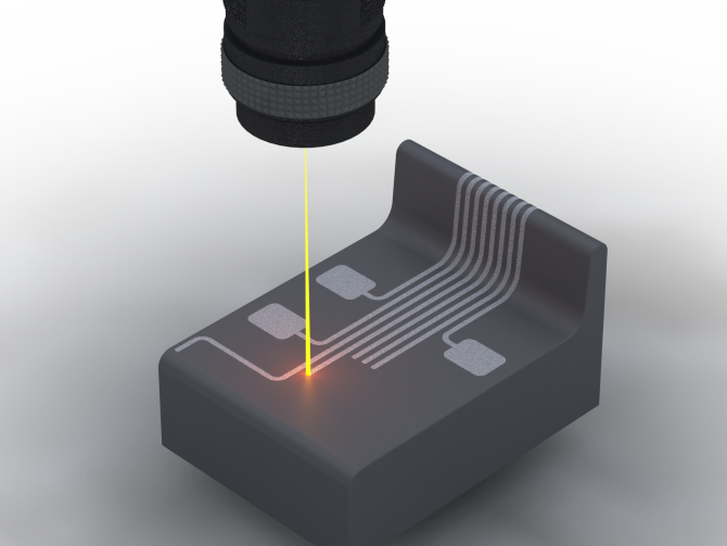
LDS allows electronic assemblies to be produced in flexible geometric styles. Clever telephones, hearing aids and good watches are turning into smaller sized and far more impressive thanks to this course of action. Supply: Harting
The additives in the content are “activated” by direct laser structuring so that the plastic material can accommodate the electrical conductor paths. The laser beam writes the spots supposed for the conductor paths and generates a micro-rough composition. The produced metal particles kind the nuclei for the subsequent chemical metallisation. In this way, the electrical conductor paths are applied to the locations marked by the laser. The other places of the a few-dimensional base human body keep on being unchanged. The plastic component can then be assembled in standard SMD procedures identical to a regular PCB. It is also ideal for soldering in a reflow oven.
Multipurpose application of laser technologies
As a single of the largest suppliers of 3D-MID factors exterior of Asia, HARTING employs higher-general performance laser techniques for the LDS procedure, with a few lasers doing work in parallel, every offset by 45 degrees. Thanks to an supplemental axis of rotation, parts can be processed by the laser at the same time from all sides (360 levels). This engineering enables flexible geometric styles, this sort of as reflector shells or LED lights, to be designed. In spite of the small conductor path thickness of 16 to 20 μm, the conductor paths are nevertheless suited for demanding automotive parts or for programs with currents up to 10 A – for instance for heating coils in cameras which are employed to avert the optics from fogging up
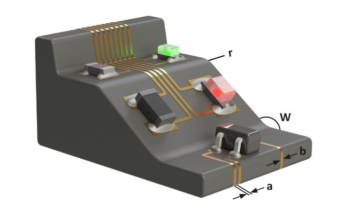
Minimal distances amongst the conductor paths (a): 50 – 150μm. Minimum amount width of the conductor paths (b): 50 – 150μm Radius (r): .2mm. Source: Harting
Frequent adjustments for the duration of the electronics growth period or new elements with modified dimensions can guide to pricey changes throughout common PCB production. The laser structure, in contrast, can be tailored pretty flexibly by applying the parameters of the laser’s handle computer software. No modifications in the injection moulding are essential for this.
The manufacturing of prototypes utilizing LDS is also simpler when compared to standard processes. HARTING can create the plastic foundation physique applying LDS-suitable substance and 3D printing. Injection moulding can also be used with cheap prototype instruments.
New developments in the LDS process
Numerous aspects of LDS technological know-how have been enhanced and even further made over the previous number of several years.
- The doing the job space of the laser has been enlarged from 160 x 160 x 80 mm to 200 mm x 200 mm x 80 mm, as a result enabling a bigger packing density and the processing of even much larger components.
- The performing velocity of the laser can be doubled to 4 m/s by optimizing the servo units and mirrors which guideline the laser beam, thus substantially decreasing the processing time.
- The improvement of the optics permits the use of a laser with a diameter of 100 μm and a laser with a good emphasis of 50 μm for processing even lesser constructions.
HARTING is the only 3D-MID maker in the globe that has a laser process with 3 fine concentration optics of 50 μm. Even smaller sized conductor path gaps can be accomplished thanks to this fine focus laser. So, a lot of conductor paths can be developed on the same element and a greater packing density can be implemented. This is employed for protection technology, between other points, due to the fact the closely spaced and intertwined conductors are able of triggering safety alarms from even the smallest actual physical interference.
Developments in elements and economics
Only specifically chosen thermoplastics are certified for the LDS process these are out there from inventory. The procedure can be even further enhanced with purchaser-certain changes to the plastic substance:
- HARTING utilizes a procedure which adds LDS additives to non-licensed supplies to make them MID-suitable.
- Unique RAL or Pantone colours can be obtained with MID plastics by employing colour pigments and specific LDS additives.
- By picking out suited additives, special RF characteristics can also be executed, based on the frequency assortment.

Digital factors – these types of as LEDs, ICs, photodiodes and sensors – can be attached immediately onto the ingredient provider. The assembled element carriers can then be processed as common SMD elements. Source: Harting
To even further increase the cost-usefulness of the producing process, HARTING depends on automated robotic techniques. The LDS laser program is outfitted with a rotary indexing desk so that a element can be inserted or taken out although a further element is nonetheless currently being processed. The in-feed and unloading treatments are automatic by HARTING employing robotics. This improves throughput and autonomy, whilst also enabling integration into automated output processes. An more automation step is supplied for the duration of the injection moulding procedure. Here, way too, a robotic can take more than the removing of the injection moulded elements. The use of robotics also improves the precise reproducibility of the procedures and, therefore, in general product good quality.
Extra expansion for 3D-MID
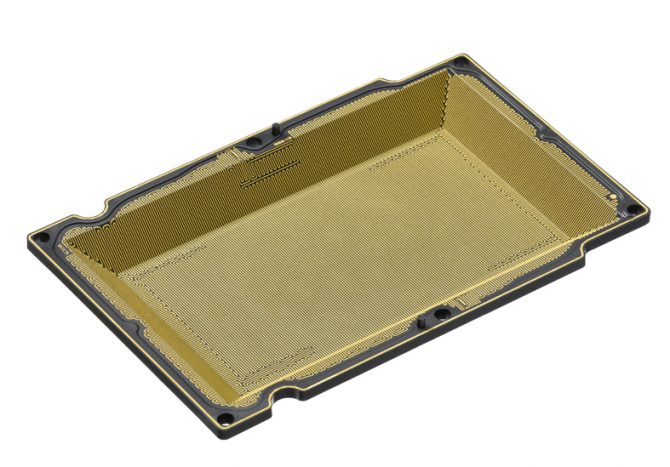
The 3D-MID caps safeguard the electronics from unauthorized access each mechanically and electronically. A highly specific meandering structure detects each access, no matter how tiny, and therefore helps prevent theft. Supply: Harting
HARTING reports improved demand for MID tasks and has additional expanded the 3D-MID division by investing in equipment and by getting a competitor’s enterprise. Ground breaking in-household solutions are also contributing to even further expansion. HARTING has developed a answer primarily based on 3D-MID technological know-how which replaces adaptable PCBs with a part carrier. As an alternative of applying a flex-PCB, the ingredient provider can be equipped straight with electronic components, as a result saving up to two thirds of the cost.
—————————————-
About HARTING 3D-MID
HARTING 3D-MID is presenting the complete price chain for 3D-MID technologies from a single supply, including progress/prototyping of purchaser-certain items, injection moulding, laser direct structuring, metallization, assembly and connection engineering, as properly as final inspection. Its main organization is the output of mechatronic elements for auto manufacturing, sector, professional medical technologies and sensor devices.
Dirk Rettschlag, undertaking manager & IE MID at Harting MID.
More Stories
US AI Industry Growth Surges: What You Need to Know
Inside the AI Boom: How the US is Leading AI Development
3 Major Advantages Of Technological Innovations